


’ 오픈")


![[정종철] 뚜따에 진심인 형+과학자코스프레+현미경을구입했어
CPU 뚜따 교육자료ㅋㅋ](https://raptor-hw.net:42215/xe/files/thumbnails/739/203/241x165.crop.jpg "뚜따에 진심인 형+과학자코스프레+현미경을구입했어")


A co-leader of Advanced Micro Devices’ central engineering group said that the company was quite satisfied with its first so-called accelerated processing unit – a chip that features both x86 processing core as well as graphics processing core – code-named Llano.
“We are quite happy with what we are seeing so far and believe that ‘Llano’ is really going to demonstrate the power of AMD’s two strengths: x86 CPUs and GPUs. The current schedule is for 2011 introduction so it is still early, but because we are using an existing CPU core for the first product and not making big changes in the memory structure right away, we feel quite confident about where we are with Llano,” said Chekib Akrout, corporate vice president of central engineering at AMD.
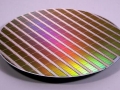
So far the information about Llano has been quite sketchy, but in case the details are summarized, the APU will seem to be quite an interesting solution for entry-level market: it will feature up to four Shanghai/Phenom II-class cores; 4MB of L3 cache; PC3-12800 (DDR3 1600MHz) memory controller, possibly, with some tweaks to better serve x86 and graphics engines; DirectX 11 graphics core with third-generation universal video decoder; PCI Express 2.0 bus for external graphics cards. What is even more interesting is that Llano appears to be a monolithic chip combining both x86 and graphics cores.
“We are doing the smart thing by taking an iterative step as we begin to tackle some of the more interesting optimizations possible with the two different types of cores,” Mr. Chekib added without elaborating.
AMD’s code-named Llano processor will be made using 32nm process technology, according to AMD’s roadmap; though, it is currently unclear whether this will be a bulk manufacturing technology, or a SOI fabrication process. Moreover, since Globalfoundries, which makes chips for AMD, will have 28nm bulk fabrication process in 2010, the chip designer may at least consider this technology in order to make the Llano chip less power hungry. Since AMD’s processors are made using SOI process, whereas the company’s ATI Radeon graphics chips are produced utilizing bulk technology. Therefore, the company will still have to redesign either in order to create the first chip that fuses AMD’s and ATI’s technologies.
As co-leader of AMD’s central engineering group, Mr. Chekib has direct responsibility for AMD’s accelerated computing efforts, research and advanced development labs (RADL), processor cores and foundational IP, CAD and layout teams.
http://www.xbitlabs.com